Soitec : News - Page 2
Cours temps réel: 43,29 0,79%| Cours | Graphes | News | Analyses et conseils | Société | Historiques | Vie du titre | Secteur | Forum |

Sur les forums on rencontre des smicards et des millionnaires. Pas besoin d'aller aux USA pour rencontrer de grosses fortunes.
Il y a des membres qui ont la capacité d'envoyer des ordres de 10 millions € voir plus.
|
Répondre
|
@Rollier1
Peut-être auriez-vous l'obligeance de m'expliquer ce que vous voulez dire ?
Téléphone au banquier, application bancaire, téléphone ou PC ou minitel, qu'importe le vecteur.
The hard fact est que le marché Euronext n'est ouvert qu'entre 08h55 et 17h35 Paris time.
Toute "solution" de type 24/24 proposée par votre prestataire préféré c'est simplement du marketing coûteux.
|
Répondre
|
« Le marché Euronext sur lequel Soitec opère, est fermé en dehors de la plage 08H55-17h35. Paris time. »
C’est ce que je t’ai dit le 12 février à 8H37 ici même. Je ne l’ignorais donc pas.
Quand je parle de « trading à la papa », je parle de ton délire de coups de téléphone aux banquiers pour acheter/vendre un titre. J’ai cru que tu plaisantais ; j’ai des doutes maintenant ! 🤔
|
Répondre
|
@Rollier1
Je vous prie de noter qu'il n'y a que le trading de Papa qui fonctionne.
Ne soyons pas trompé par des "solutions de trading" qui ne peuvent pas contourner un hard fact :
Le marché Euronext sur lequel Soitec opère, est fermé en dehors de la plage 08H55-17h35. Paris time.
|
Répondre
|
Pêcher à la dynamite dans une mer vide de poissons ne fait remonter plus de poissons, ça finit juste de détruire l'écosystème qui a prévalu jusqu'à présent…
|
Répondre
|
« Il est malaisé pour un acheteur à Denver de téléphoner à 3 heures du matin à un banquier du Crédit Agricole, chez qui il n'a pas de compte, pour lui demander d'acheter du Soitec »
Ça, c’est du trading de papa ! 🤪
|
Répondre
|
Excellente remarque, je vous en remercie.
Le phénomène que vous décrivez reste toutefois parfaitement anecdotique : Il est malaisé pour un acheteur à Denver de téléphoner à 3 heures du matin à un banquier du Crédit Agricole, chez qui il n'a pas de compte, pour lui demander d'acheter du Soitec.
En pratique, le gars de Denver appellera à 08h30 heure locale (16h30 Paris) son banquier habituel à la First Interstate (installée sur Wazee street), banquier qui passera un ordre d'achat sur Soitec via le système informatique du Crédit Agricole (canmp.fr), correspondant en France de la First Interstate.
Dans un deuxième temps, après exécution de l'ordre, le banquier de la First Interstate transfèrera le cash du paiement des Soitec du gars de Denver, sur le compte dit "nostro" du Crédit Agricole à la First.
Puis le Crédit Agricole créditera alors le compte titre "loro" de la First chez eux, du nombre d'actions Soitec correspondante, sans connaitre l'identité du gars de Denver.
Le principe est le même que le gars de Denver soit un individuel ou un fonds de pension.
|
Répondre
|
Les Américains n’ont pas besoin d’attendre l’ouverture de N.Y. pour acheter sur le marché français. Ils peuvent le faire dès que le marché français est ouvert.
|
Répondre
|
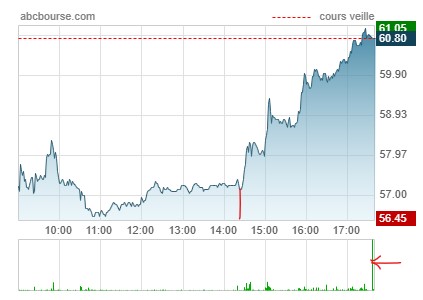
Bonjour amis investisseurs de Soitec,
L'évolution du cours d'hier montre qu'un transfert de propriété de la société est en cours vers des investisseurs américains.
On voit sur le graphique qu'à 14h30 (ouverture de NY) un flux d'achat américain a remplacé le rythme de stagnation européen du matin. Flux d'achat très régulier (+5% en ligne droite) et très puissant (1,30% du capital échangé au final).
Soit un transfert net d'environ 0,13% du capital de portefeuilles européens vers des portefeuilles américains (Rule of thumb : 10 allers-retours "techniques" pour un aller simple "économique").
80,000 actions échangées en 5 minutes à la clôture, sans impact significatif sur le cours (c'est à dire +/- nb ventes = nb d'achats), c'est énorme.
Difficile de dire que les Américains en sauraient plus que les Français sur une société iséroise. Mais ca dit probablement quelque chose sur notre aversion collective au risque.
|
Répondre
|
Eh bien, si une « ultimate proof » n’est pas nécessaire, pourquoi t’évertues tant sur le sujet ? 🤔
|
Répondre
|
La journée d'hier pour le secteur des Semis est la "ultimate proof" de l'inanité de toute "analyse" fondée sur la forme de la courbe du cours.
Si tant est qu'une ultimate proof soit nécessaire :
|
Répondre
|
Hi ! Hi Hi !
Persister dans ses erreurs n’est pas une preuve d’intelligence 🙄
|
Répondre
|
La journée d'aujourd'hui pour le secteur des Semis est la "ultimate proof" de l'inanité de toute "analyse" fondée sur la forme de la courbe du cours.
Si tant est qu'une ultimate proof soit nécessaire :
|
Répondre
|
Soitec bondit, les investisseurs sont rassurés par les perspectives liées à l'IA
Le 05 décembre 2024 à 16:04
PARIS (Agefi-Dow Jones)--Le titre Soitec bondit de 12,1%, à 84,65 euros, jeudi alors que le fabricant de matériaux avancés pour l'industrie des semi-conducteurs accueillait mercredi à Santa Clara, en Californie le "Substrate Vision Summit", un événement consacré au rôle des matériaux semi-conducteurs dans le développement de l'intelligence artificielle (IA). Selon un analyste parisien, cette journée de présentation a sans doute permis aux investisseurs de mieux intégrer l'impact positif de l'IA sur l'activité de Soitec, notamment pour équiper les centres de données qui doivent répondre à la croissance exponentielle des besoins en capacités de calcul liés à l'IA. Dans ce cadre, le marché pourrait être rassuré au sujet des perspectives de croissance du groupe à moyen terme, précise l'expert.
Par ailleurs, CM-CIC Securities a commencé jeudi le suivi du titre avec une recommandation "achat" et un objectif de cours de 120 euros.
|
Répondre
|
Retour en pullback sur l'ancien point bas (+ comblement du gap un poil + haut)
mais après ? O_o
en attendant, on a le droit aux rachats de short ! 
|
Répondre
|
A l'occasion de la publication des résultats semestriels de Soitec , Pierre Barnabé, directeur général du leader mondial dans la production de substrats pour galettes à semi-conducteurs, était l'invité de l'émission Ecorama du 25 novembre 2024, présentée par David Jacquot sur Boursorama.com. Parmi les sujets abordés : la diversification du portefeuille d'activité, la montée en puissance de l'IA, et le cours de Bourse.
|
Répondre
|
Rendez-vous à Santa Clara le 4 Décembre :
https://semiwiki.com/events/350542-i-will-see-you-at-the-substrate-vision-summit-in-santa-clara/
As the demand for faster, smaller, and more efficient electronic devices continues to surge, the role of advanced semiconductor materials becomes increasingly critical. This conference will delve into topics such as the latest breakthroughs in silicon-based technologies, the rise of alternative materials like gallium nitride (GaN) and silicon carbide (SiC).
|
Répondre
|
Bonjour amis investisseurs dans Soitec,
Le communiqué d'hier de Soitec a été plutôt rassurant. Pour 2 raisons :
- Le point bas de commandes semble passé
- La société reçoit suffisamment de stimulus de la part de clients déprimés pour maintenir ses investissements
On ne peut évidemment pas considérer les 8% d'augmentation d'hier comme une inversion de tendance encore.
Mais je pense que l'affirmation du président "on a passé le point bas [économique]" n'est pas que de méthode Coué.
|
Répondre
|
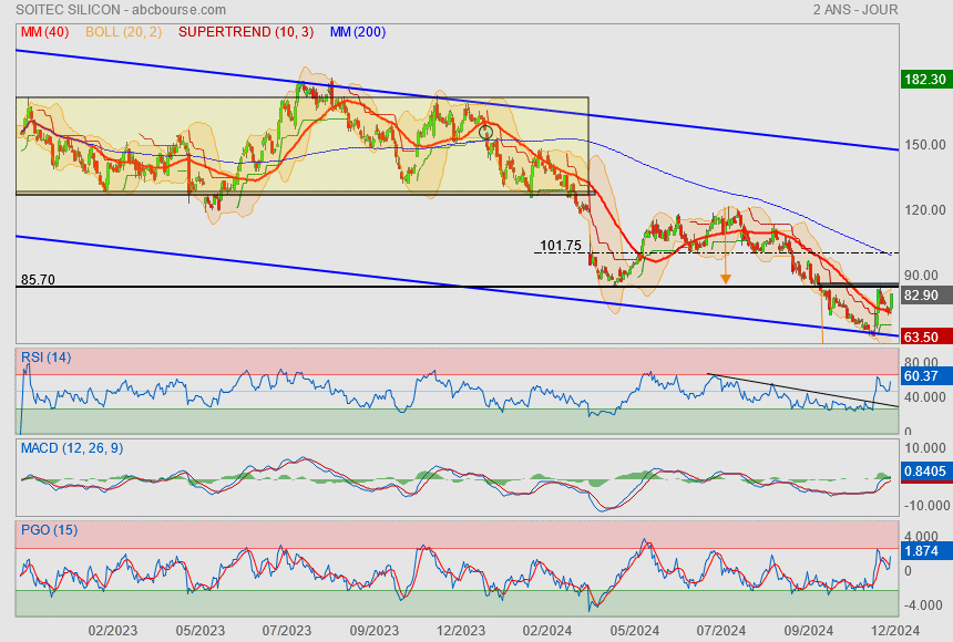
Puisqu'on est rendu à 64,10€ actuellement et que voilà rendu aux oubliettes de cul de basse-fosse…
Et qu'on fait -60,48% depuis le 1er janvier 2024…
Je vous profite pour retourner le message que vous aviez posté au sujet de mes graphes baissiers de Soitec le 10 Mars 2024 à 14 h 25.
https://www.abcbourse.com/forums/msg1007723_soitec-plus-pessimiste-sur-ses-objectifs-annuels
"Bonjour,
J'ai exactement la bonne vidéo pour vous aider à comprendre pourquoi vous ne pouvez pas être un expert du futur du cours de Soitec.
Regardez ce Veritasium je vous propose, il est véritablement très instructif :
https://www.youtube.com/watch?v=5eW6Eagr9XA
Je suis sincèrement désolé."
|
Répondre
|
What are the recent progress of the four major FD-SOI manufacturers?
Posted on 2024-10-26
Author: Liu Yuwei, deputy chief analyst of Electronic Engineering Journal share
The current major players in global FD-SOI technology include Soitec, GlobalFoundries, Samsung Electronics, STMicroelectronics and other companies. They have invested a lot of resources in the research and development and commercialization of FD-SOI technology. What is the current progress of the industry?
FD-SOI (Fully Depleted Silicon-on-Insulator) is an advanced semiconductor manufacturing process that combines a planar transistor structure with fully depleted operating characteristics. This technology relies on a unique substrate with an ultra-thin top silicon layer and buried oxide layer (BOx), which enables better gate control and lower leakage current. Compared with traditional bulk silicon CMOS processes, FD-SOI provides significant advantages at 28nm and below nodes, including higher performance, lower power consumption, and better RF performance.
These advantages of FD-SOI technology make it more suitable for low-power devices such as mobile and IoT . In particular, its fully depleted and highly integrated characteristics make FD-SOI advantageous in RF applications and cost-sensitive systems that require multiple functional integration, such as smart devices, 5G communications, and automotive radars.
Currently, FD-SOI has achieved growth in several key application areas, including smartphone devices, IoT, data centers and infrastructure, and the automotive industry. These applications include millimeter wave front-ends, display driver integrated circuits (DDICs), security elements, wireless microcontrollers (MCUs), edge artificial intelligence, human-machine interfaces (DDICs, ISPs), satellite communications and wireless infrastructure, optical network transceivers, smart sensors (ISPs, radars), and automotive processing (MCUs).
The global FD-SOI market has experienced significant growth in the past few years, mainly due to the increasing demand for low-power and high-performance chips. According to market research reports, the global FD-SOI market size is approximately US$690 million in 2022 and is expected to grow at a compound annual growth rate of 34.5% to reach approximately US$4.09 billion by 2027.
The main players in the current global FD-SOI technology include Soitec, GlobalFoundries, Samsung, STMicroelectronics and other companies, which have invested a lot of resources in the research and development and commercialization of FD-SOI technology. At the 9th Shanghai FD-SOI Forum held recently, many manufacturers' representatives discussed in depth the design techniques, industry chain status and market development trends of the technology, and shared a number of successful application cases.
GlobalFoundries: 12nm FDX® expected to be launched in 2026
Hong Qicai, President of GlobalFoundries Asia and Chairman of GlobalFoundries China, shared the company's progress in the field of FD-SOI technology and the roadmap for future innovation. It is reported that GlobalFoundries' GF 22FDX® platform provides ultra-low power consumption, excellent RF performance, integrated non-volatile memory (including MRAM and RRAM), and intelligent and secure features. These features make 22FDX® an ideal choice for automotive, consumer electronics, industrial applications, and low-power IoT and mobile applications.
Hong Qicai, President of GlobalFoundries Asia and Chairman of GlobalFoundries China
Starting with the launch of 22FDX® in 2015, GlobalFoundries' FD-SOI technology roadmap has continued to evolve, and the now launched 22FDX+ will achieve half-node power scaling, providing 22% lower power consumption. Hong Qicai said, "Our 22FDX® has been put into production at the Dresden plant in Germany, and part of the production capacity has been transferred to the Malta plant in New York. In the next two years, we will continue to improve our embedded MRAM and RRAM according to customer requirements with the goal of reducing costs, and realize integrated non-volatile memory, which is planned to be launched between 2025 and 2028."
It is reported that GlobalFoundries' next-generation FD-SOI roadmap will push the current 22FDX technology into 12nm FDX technology. This generation of technology will focus more on automotive applications, such as image signal sensors (ISP) and radars, as well as automotive control system MCUs, and will introduce built-in automotive quality processes AutoPro.
In the field of IoT, GlobalFoundries will achieve significant volume and cost benefits by introducing FD-SOI into display drivers. Hong Qicai believes that this will provide the company's FinFET products with more stable performance at the 28nm node, which is especially important for AMOLED drivers.
In the field of millimeter wave, GlobalFoundries has launched an important program in Dresden to achieve fT/fMax RF performance of more than 500GHz (>500GHz fT/fMax). This is also a key technology to drive the next generation of FDX, which will cover the frequency range from 1GHz to 300GHz and is suitable for applications such as satellite communications, automotive radar, 6G JCAS, gesture sensing and high-speed interfaces.
"12FDX technology provides full-node PPA scaling and offers improved architecture and IP optimized for AI MCUs, simplifying migration from 22FDX. It will not only reduce the size, but also improve energy efficiency and performance." The technology is suitable for applications that require higher numbers, more AI/ML, 7nm-like low power consumption and high RF capabilities. Hong Qicai expects this technology to be launched in 2026 .
In addition, it was revealed that some of GlobalFoundries' customers are using 22FDX for 3D stacking, using GlobalFoundries' wafers as the base SOC and stacking gallium nitride (GaN) and micro-LEDs on them. This will expand the company's 12nm and 22nm FD-SOI process wafer usage.
Currently, GlobalFoundries is also developing 3D high-density interconnect (3D HI) technology through TSV, W2W/D2W and silicon interposer solutions. This technology can reduce chip size by up to 45%, providing expansion possibilities for valuable board space on mobile devices while also increasing the application scope of 22FDX and 12FDX.
Samsung: Why do we need to use 18nm FD-SOI process?
Samsung's history in FD-SOI technology can be traced back to its collaboration with STMicroelectronics. After STMicroelectronics developed the 28nm FD-SOI process (28 LPP), the technology was transferred to Samsung and eventually brought to market.
Jinha Park, process integration and project manager of Samsung Electronics 18FDS, said that Samsung did not stop at the development of FD-SOI technology, and subsequently continued to develop a number of derivative products covering automotive and mobile applications. In order to further promote the development of FD-SOI technology, Samsung decided to develop the next generation of FD-SOI technology, namely 18FDS.
Jinha Park, Process Integration and Project Manager, 18FDS, Samsung Electronics
Samsung now has 35 28nm FD-SOI technology products in mass production and application, with stable output and gradually improved yield (DO). Samsung has also developed a series of advanced derivative processes for applications in RF/Auto/NVM (eMRAM) and automotive fields. Jinha Park focused on the eMRAM technology, which is the world's first commercialized 28nm Flash-type eMRAM with a stable yield of over 98%.
According to reports, Samsung and STMicroelectronics worked closely together to overcome many technical challenges when developing 18FDS technology. In 2017, STMicroelectronics proposed to jointly develop FD-SOI process MCUs with Samsung, which was an important milestone in the cooperation between the two parties. Jinha Park said, "We reviewed the previous FD-SOI technology and solved some problems in the new generation of technology, including process improvement and BEOL, to launch 18FDS."
Samsung's 18nm FD-SOI key processes include CPPs, TGO (Triple), eZG (0.35um) _Native, MEO and BEOL. The figure below shows the process stack (8ML) and support for low-temperature BEOL. The table lists the SG suite, DRAM bit-cell, EG suite and eZG suite, as well as their main parameter characteristics.
Jinha Park emphasized several key features of 18FDS technology, including eZG 3.3V (Native), mixed standards (L/R/HVT), support for ultra-low power devices, high-performance RF units and digital processors, and also demonstrated performance, power and area (PPA) analysis and high voltage (3.3V) and high-speed analog support, as well as small standard units and low power consumption. Compared with the previous 28nm FD-SOI, 18FDS technology has significantly improved performance, power consumption and area (PPA).
In addition, he also introduced the easy-to-port NVM solution of 18FDS. Jinha Park believes that the native 3.3V and low leakage characteristics of 18FDS technology will not only be widely used in smartphones and mobile devices, but will also become an important platform in the fields of IoT and automotive electronics. "We expect that 18FDS will play a key role in future high-performance computing and communication applications. It will enter the IP construction and verification stage in 2025."
STMicroelectronics: Application prospects of FD-SOI technology
"STMicroelectronics has been a pioneer in FD-SOI technology since 2012 and has driven the development of this technology together with partners such as Samsung and GlobalFoundries." John Carey, Director of RF and Communications Division at STMicroelectronics, discussed the unparalleled advantages of FD-SOI technology in low-power applications, RF characteristics, and the cost-sensitive market of embedded non-volatile memory (eNVM) at the meeting.
John Carey, Director of RF and Communications Division, STMicroelectronics
It is reported that the technical advantages of FD-SOI mainly include the following points:
Low Power Mode
Intelligent low-power mode : Using forward body biasing technology, the platform can be turned off when not in use, significantly reducing energy consumption. Compared with traditional platforms, it can save up to 99% of power consumption.
Static process control : FD-SOI technology provides another mechanism to control process parameters by adjusting bias to tune performance at low temperatures and reduce leakage current at high temperatures, thereby improving yield and stability.
2. Soft Error Rate
Reliability : FD-SOI technology significantly reduces the soft error rate, which is particularly important for automotive design. Through design, FD-SOI technology can reduce the soft error rate to 1/100 of that of ordinary CMOS processes, thereby improving reliability.
3. RF performance and analog integration
RF Performance : In addition to digital performance, the FD-SOI platform offers improved analog performance, including highly efficient short devices, large tuning range, and high-performance high-frequency behavior.
Analog Blocks : All analog blocks have improved speed, higher gain for a given current density, lower gate and parasitic capacitance, less noise variation, and better matching. These features are unique to planar processes and cannot be achieved in discrete FinFETs.
John Carey emphasized the application of FD-SOI technology in automotive electronics, especially in automotive-grade MCUs, ISPs, and radar sensors. "STMicroelectronics is developing 18nm FD-SOI technology with embedded PCM memory, which is particularly suitable for systems that require high reliability."
Finally, John Carey looked forward to the future development of FD-SOI technology, especially its expansion in automotive electronics and industrial embedded applications. He said that STMicroelectronics will continue to work with its partners to promote the development of this technology and expressed great interest and expectations for the potential of the Chinese market.
Soitec: How FD-SOI substrates serve the AI and automotive industries
The substrate is one of the most important materials in the semiconductor industry, especially the FD-SOI substrate, which has unique advantages in improving device performance, reducing power consumption and integrating RF functions. Soitec uses Smart Cut™ technology to achieve thickness uniformity, roughness, new material application and defect control of silicon wafers, thereby improving the performance and reliability of semiconductor devices.
In his speech, Philippe Flatresse, Product Marketing Manager at Soitec, discussed how FD-SOI technology can add value to the semiconductor industry and highlighted the application prospects of FD-SOI technology in edge AI and automotive fields.
Philippe Flatresse, Product Marketing Manager at Soitec
In his opinion, the advantages of FD-SOI substrates include the following:
Performance Advantages
High performance : FD-SOI substrate provides higher transconductance (Gm) and cutoff frequency (Ft/Fmax), thereby improving transistor performance.
Low power consumption : Through thin buried oxide layer and reverse body bias technology, FD-SOI substrate can significantly reduce leakage current and achieve lower power consumption.
High integration : FD-SOI technology can integrate digital, analog, and RF modules on a single chip, reducing system size and cost.
2. RF performance
Low noise : FD-SOI transistors have lower gate capacitance and resistance, which reduces noise.
High Linearity : Undoped silicon channel provides better linearity for high power applications.
High reliability : FD-SOI technology improves system reliability and stability and reduces soft error rate.
3. Cost-effectiveness
Easy integration : FD-SOI technology simplifies the integration of digital/analog/RF modules, reducing design complexity and cost.
Efficient computing : FD-SOI technology supports flexible computing, which enables devices to adjust performance based on demand, thereby improving energy efficiency.
Philippe Flatresse analyzed the market drivers of FD-SOI technology, including high-performance computing, green energy and mobility. He mentioned that the advantages of FD-SOI technology in high performance, low power consumption and high integration make it an ideal choice for edge AI and automotive applications.
In terms of edge AI, FD-SOI technology supports battery-powered high-performance computing, which is suitable for applications that require real-time processing; it integrates RF modules to support wireless communications; it integrates non-volatile memories such as MRAM and RRAM, providing an important storage solution for edge computing.
In automotive electronics, FD-SOI technology is particularly used in image signal processors (ISPs) and radar sensors, which improve the perception capabilities of automotive systems. When used in automotive microcontrollers (MCUs), it can improve the overall performance and reliability of the system. When used in regional controllers for next-generation smart vehicles, it can achieve more efficient wireless connectivity and control.
Regarding FD-SOI substrate production capacity, it is reported that Soitec's Bernin 2 plant in France has increased its maximum capacity from 650,000 wafers per year to 700,000 wafers per year; the plant in Pasir Ris, Singapore has also reached a maximum capacity of 1 million wafers per year. In addition, Soitec is developing new substrate technologies, such as eSOC 3, to further improve performance and energy efficiency.
Conclusion
The investment and R&D of these international leading companies in the FD-SOI field have not only accelerated the maturity of the technology, but also promoted the commercialization of related products and solutions.
In China, FD-SOI technology is also highly valued. The support of the government and the technological progress of local enterprises have jointly promoted the rapid development of this technology in China. VeriSilicon and Huali Microelectronics are actively exploring and adopting FD-SOI technology for the design and production of IoT chips. Shanghai Fudan Microelectronics, Hunan Guoke Micro and many other Chinese companies are also actively promoting the application and development of FD-SOI technology.
Looking ahead, FD-SOI technology has broad prospects for development. With the continuous advancement of technologies such as 5G, artificial intelligence, and autonomous driving, the demand for high-performance, low-power semiconductor solutions will continue to grow. With its unique advantages, FD-SOI technology is expected to occupy an important position in the future semiconductor market, lead the technological trend, and bring new growth points to the global electronics industry.
|
Répondre
|
Forum de discussion Soitec Silicon
202502131703 1027879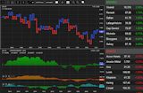 Suivez les marchés avec des outils de pros !